AI Tools Speed Semiconductor Fab Simulations and Process Decisions
- Gate
- Machine Learning
- Departs
- Crew
- Timothy Costa
- Passengers
- 760
Faster simulations, physics based predictions, task agents and fab digital twins give engineers more ways to assess changes before physical trials.
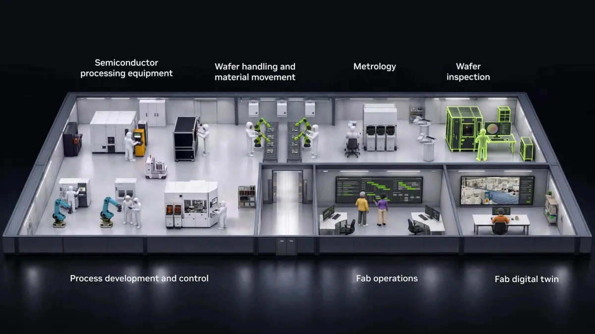
AI is changing the pace of semiconductor engineering by helping teams evaluate process changes before they commit to expensive fab trials. The tools described here speed up simulations, predict some physical behavior without rerunning full models, automate selected engineering tasks and let teams test factory changes in digital twins. Their value lies in giving engineers more chances to compare options while keeping technical decisions in human hands.
That matters as chip manufacturing grows more complex and the margin for process error narrows. Assessing how a material responds to a new step, tracing a defect to its cause, or estimating the effect of a process adjustment can take days. Physical trials consume time and fab capacity, and a mistaken assessment of yield or process quality can have costly consequences. Faster analysis can change which questions engineers have time to investigate before acting.
More simulation runs before a physical trial
Accelerated computing can shorten individual calculations, but the larger benefit is that engineers may compare more alternatives within the same time. Multiphysics models account for interactions among effects such as heat transfer, electrical behavior and mechanical stress. Those interactions matter when engineers assess equipment and process settings, but they can make simulation computationally demanding.
COMSOL, a multiphysics software provider, reports that the NVIDIA cuDSS library can accelerate relevant semiconductor manufacturing simulations by up to 10x. The additional capacity can help engineers compare process options and decide which changes merit physical testing. The reported figure describes acceleration for these simulations; it does not by itself establish how much a fab’s yield or throughput will improve.
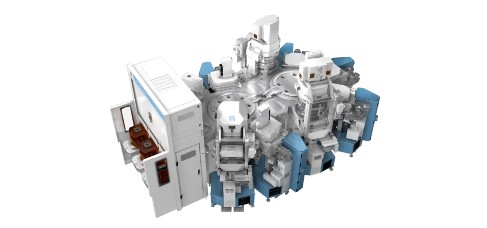
Applied Materials is also applying cuDSS to its Ginestra simulation platform, which models materials at atomic scale. The platform runs up to 10x faster than CPU only approaches, according to the source. Its ACE+ multiphysics platform uses NVIDIA PhysicsNeMo for topography simulations, with acceleration of up to 35x. These results point to a practical use for computing capacity: examining material behavior and process outcomes across more scenarios during development.
Some calculations are so demanding that speed changes whether they can be used at production scale. Computational lithography models how circuit patterns will print onto silicon. Siemens is integrating NVIDIA cuLitho into its Calibre lithography software, with up to 17x acceleration on key simulation workloads. That can expand the set of patterning cases engineers are able to verify before a wafer reaches the printing stage.
Physics based AI can reduce repeated full simulations
Faster hardware still leaves a tradeoff: complex physical simulations can remain expensive to run repeatedly. AI models trained on physics offer another route, predicting how a material or process may behave without executing a full simulation for every new condition. The prediction is useful as a way to explore possibilities quickly; it does not remove the need to validate important results against detailed models or experiments.
Plasma etching illustrates the challenge. Plasma is an electrically charged gas used to remove material during chip fabrication. Modeling it means accounting for interacting electrical, chemical and thermal effects. Lam Research demonstrated that the NVIDIA PhysicsNeMo framework can predict plasma behavior in milliseconds, compared with days for a full simulation. That difference could let engineers screen process conditions more quickly and reserve the costlier calculation for cases that warrant closer examination.
Agents take on selected engineering steps
Engineering work involves more than choosing a final process setting. Teams also have to investigate failures, compare tools and models, and carry out the steps that inform a decision. AI agents can handle some of that intermediate work, though the example here concerns a specific task rather than autonomous fab operation.
Advantest uses agents built with NVIDIA NeMo Switchyard to select which AI model to apply to a task. The source describes this model selection as a manual process that can take hours on the test floor; the agents reduce response times to minutes. That may shorten one part of an engineering workflow, while engineers remain responsible for interpreting results and deciding what to change.
Digital twins bring factory level changes into simulation
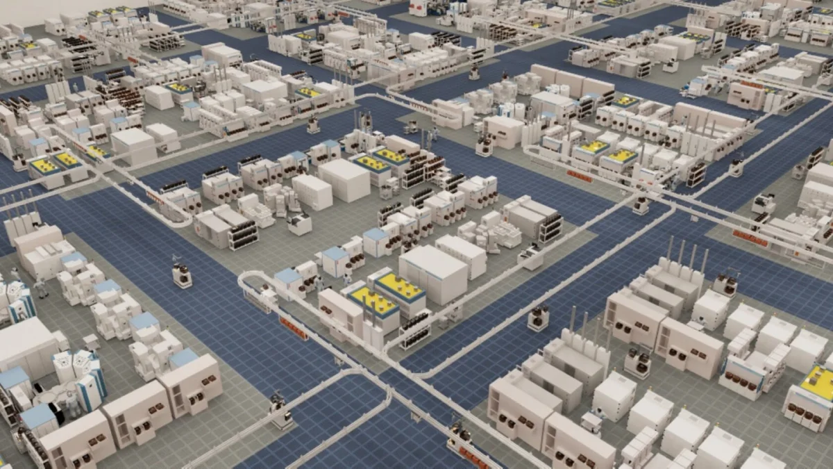
Digital twins extend virtual testing from individual process steps to equipment arrangements and the movement of materials through a factory. Teams can use them to evaluate layouts, look for bottlenecks and consider operating strategies before making physical changes. As fab layouts and process dependencies grow more involved, testing those interactions virtually can help teams spot problems earlier.
Applied Materials uses NVIDIA Omniverse libraries to build physically accurate digital twins of entire fabs. The models can simulate material movement and support evaluation of layout and operating choices. A fab level twin gives teams a way to examine how a change in one area could affect factory operations elsewhere, although its usefulness depends on how well the virtual model represents the physical site and its processes.
Connecting predictions to production decisions
These capabilities become more useful when production data informs models, models help assess proposed changes, and the findings return to the engineers responsible for process decisions. In that loop, accelerated simulation can explore alternatives, physics based AI can provide faster estimates, agents can handle defined tasks, and digital twins can test broader factory effects.
The source describes an AI defined fab as a factory where AI helps optimize processes, identify problems earlier and inform decisions across chip manufacturing. The concrete examples show speedups and shorter response times for particular tools and tasks; they do not establish a single performance gain across every fab. The measure to watch is how well these systems connect to real production data and help engineers make better decisions before committing to changes on the line.